Coal-derived carbon nanodots are emerging as a compelling bridge between abundant carbon resources and advanced nanoscale electronics. By turning coal into ultra-small, tunable carbon nanomaterials, researchers can explore new ways to improve 2D devices built from atomically thin materials. The opportunity is not simply to make electronics smaller, but to make interfaces cleaner, charge behavior more controllable, and material platforms more practical for future manufacturing.
Why do coal-derived carbon nanodots matter for 2D electronics?
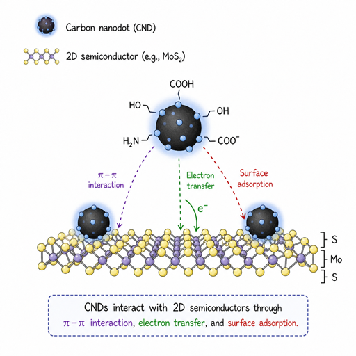
Coal-derived carbon nanodots matter because they offer a nanoscale carbon platform with useful optical, electrical, and surface-chemistry properties that can complement 2D materials. In next-generation electronics, performance often depends on what happens at interfaces: how charges move, how defects are controlled, and how thin layers interact. Carbon nanodots can be engineered as additives, interlayers, coatings, or functional modifiers that help tune these behaviors without adding bulky structures.
This is especially relevant for 2D electronics, where materials such as graphene, transition metal dichalcogenides, and other atomically thin semiconductors are highly sensitive to their surrounding environment. A tiny amount of contamination, trapped charge, or structural disorder can change device behavior. Coal-derived carbon nanodots provide a potential route to manage those interactions with a material family that is small, chemically flexible, and compatible with solution-based processing.
From traditional carbon source to advanced nanomaterial
Coal is usually discussed as an energy resource, but it is also a complex carbon-rich material. When processed at the nanoscale, parts of that carbon structure can be transformed into carbon nanodots: small particles with dimensions typically discussed in nanometers and with surfaces that can carry different chemical groups. Those surface groups are important because they influence solubility, film formation, charge transfer, and compatibility with other materials.
The phrase “coal-derived carbon nanodots” does not refer to a single universal material. It describes a family of carbon nanodots made from coal-based precursors through chemical, thermal, or other synthesis approaches. The exact properties can vary depending on the coal source, purification method, reaction conditions, and post-treatment. That variability is a challenge, but it is also one reason the material class is interesting: researchers can tune the dots for different roles.
In electronics, tunability matters. A material used as a charge-transfer layer may need different behavior than one used as a passivation coating or sensing component. Coal-derived carbon nanodots can potentially be designed for these different functions by adjusting their size distribution, surface chemistry, and interaction with the 2D material surface.
The role of carbon nanomaterials in thinner, smarter devices
Carbon nanomaterials have long attracted attention because carbon can form many useful structures, from sheets and tubes to dots and porous networks. Each structure brings a different mix of conductivity, chemical stability, mechanical flexibility, and processability. Carbon nanodots occupy a distinct position in this landscape because they combine nanoscale size with surface-driven behavior.
For 2D electronics, that surface-driven behavior is valuable. Two-dimensional devices often rely on very thin active channels, so the surrounding layers can strongly affect the final device. A carefully selected nanodot layer may help modify local electronic environments, support better contact behavior, or protect delicate surfaces from unwanted interactions.
Carbon quantum dots, a closely related term often used for luminescent or quantum-confined carbon nanodots, also bring optical functionality into the discussion. That makes them relevant not only for transistors, but also for photodetectors, light-responsive sensors, and optoelectronic systems where electrical and optical signals are connected.
How can carbon nanodots improve 2D device performance?
Carbon nanodots can improve 2D device performance by influencing the interface between the active 2D layer and its surrounding contacts, substrates, or environment. Their small size and modifiable surfaces make them useful candidates for defect passivation, charge modulation, film engineering, and hybrid device design. The practical effect depends on how the nanodots are synthesized, where they are placed, and how they interact with the device stack.
Several possible roles stand out:
- Interface modifiers: Carbon nanodots may help tune the contact between metals and 2D semiconductors, which can affect charge injection and device consistency.
- Defect passivation layers: Their surface groups may interact with dangling bonds, vacancies, or reactive sites, reducing unwanted trap behavior.
- Charge-transfer components: Depending on their chemistry, carbon nanodots may donate, accept, or redistribute charge near a 2D channel.
- Protective coatings: Thin nanodot-based layers may help shield sensitive materials from moisture, oxygen, or processing residues.
- Optoelectronic enhancers: Carbon quantum dots can add light absorption or emission behavior, supporting hybrid photodetectors and sensor designs.
These benefits are not automatic. A poorly controlled nanodot film could introduce roughness, impurities, or unstable charge states. The most promising work will likely focus on repeatable synthesis, clean integration, and careful matching between the nanodot chemistry and the 2D material system.
Where coal-derived carbon nanodots fit in the 2D electronics stack
A 2D electronic device is more than its active channel. It includes a substrate, electrodes, dielectric layers, encapsulation, and sometimes optical or chemical sensing interfaces. Coal-derived carbon nanodots could fit into several parts of that stack, depending on the device goal.
In transistor designs, they may be explored as interfacial layers that influence how charges enter or leave the channel. In sensors, their surface chemistry could help capture specific molecules or improve signal response when the 2D layer is exposed to the environment. In photodetectors, carbon quantum dots may support light interaction while the 2D material provides fast charge transport.
A useful way to think about the opportunity is not as a replacement for 2D materials, but as a companion material. The 2D layer provides the atomically thin electronic pathway. The carbon nanodots help shape the local chemical, optical, or electronic environment around that pathway.
Practical integration pathways
Researchers and device developers may consider several integration methods:
- Solution deposition: Nanodots dispersed in suitable solvents can be deposited by spin coating, drop casting, printing, or related methods.
- Layer-by-layer assembly: Thin films can be built gradually to control coverage and reduce unwanted aggregation.
- Surface functionalization: Chemical groups can be selected or modified to improve adhesion, charge behavior, or compatibility.
- Hybrid composites: Carbon nanodots can be combined with polymers, oxides, or other nanomaterials to create multifunctional layers.
- Localized patterning: Future device architectures may require placement only in selected areas, such as contacts or sensing regions.
Each method carries trade-offs. Solution processing can be scalable, but it requires control over film uniformity and residue. Surface functionalization can improve compatibility, but it may also change electronic behavior. Hybrid composites can add useful functions, but they can make the system harder to analyze.
Advantages that make the material platform attractive
The appeal of coal-derived carbon nanodots comes from a combination of material availability, nanoscale function, and chemical versatility. Coal-based precursors are carbon-rich and widely known, while carbon nanodots are small enough to interact with modern devices at relevant length scales. This combination encourages research into whether conventional carbon sources can support advanced materials rather than only traditional energy uses.
Key advantages include:
- Resource transformation: Coal can be reimagined as a precursor for higher-value carbon nanomaterials.
- Surface tunability: Functional groups can be adjusted to influence solubility, adhesion, and charge interaction.
- Potential processability: Nanodots may be compatible with liquid-phase methods useful for coating and printing.
- Hybrid functionality: Carbon nanodots may combine electrical, chemical, and optical effects in one nanoscale platform.
- 2D material compatibility: Their small size makes them suitable for interface engineering without necessarily adding thick layers.
These advantages are most meaningful when paired with rigorous material control. For electronics, consistency is often as important as peak performance. A material that works once in a lab demonstration must eventually be reproducible across many devices and fabrication batches.
What challenges must be solved before wider adoption?
The main challenges are consistency, purity, integration control, and long-term stability. Coal-derived carbon nanodots can vary depending on the starting material and synthesis process, so electronics applications need reliable control over size, composition, surface groups, and impurities. Without that control, device behavior may become difficult to reproduce.
Purification is another major issue. Electronic devices can be sensitive to trace contaminants, and coal-based sources may contain complex mixtures that require careful processing. Any remaining impurities could affect charge transport, contact quality, or device lifetime.
There is also the challenge of understanding mechanisms. If carbon nanodots improve a device, researchers need to know whether the improvement comes from passivation, doping, morphology, optical interaction, or another effect. Clear mechanisms make it easier to design better devices instead of relying on trial and error.
Finally, integration with existing fabrication flows must be practical. Materials for next-generation electronics need to survive processing conditions, remain stable during operation, and work with scalable patterning methods. Coal-derived carbon nanodots have promise, but the path from promising material to manufacturing-ready component requires careful engineering.
Applications that could benefit first
Some applications may be better suited for early exploration than others. Highly standardized logic chips require extremely tight process control, so they may be a longer-term target. Sensors, flexible devices, and optoelectronic prototypes may offer more room for experimentation because their architectures can tolerate more material variation while still gaining useful functionality.
Potential early-use areas include:
- Chemical and biological sensors that use surface interactions to detect target molecules.
- Flexible electronics where low-temperature, solution-based processing is valuable.
- Photodetectors that combine carbon quantum dots with 2D semiconductors for light-responsive behavior.
- Memory or neuromorphic concepts where charge trapping and interfacial states can be engineered intentionally.
- Protective interface layers for stabilizing sensitive 2D materials during device operation.
In each case, the value comes from matching the nanodot function to the device need. A sensor may prioritize surface chemistry, while a transistor may prioritize clean charge transport. The same material family can support different goals when tuned with care.
A more circular view of advanced electronics materials
One of the most interesting aspects of coal-derived carbon nanodots is the shift in perspective they represent. Instead of viewing coal only through the lens of combustion, researchers can investigate whether carbon-rich resources can be transformed into functional nanoscale materials. That does not erase environmental concerns around coal extraction or use, but it does open a different conversation about material value and carbon utilization.
For the electronics industry, this matters because future devices will require not only performance, but also smarter material choices. Advanced electronics depend on complex supply chains and specialized materials. If abundant carbon sources can be responsibly converted into useful nanomaterials, they may add another option to the materials toolkit.
The sustainability case should be made carefully. A material is not automatically sustainable because it comes from an abundant precursor. Processing chemistry, energy use, waste handling, purification, and device lifetime all influence the real environmental profile. Still, coal-derived carbon nanodots invite important research into how legacy carbon resources might be redirected toward higher-value technologies.
The road ahead for coal-derived carbon nanodots
The future of coal-derived carbon nanodots in 2D electronics will depend on repeatability, integration, and proof of practical benefit. Researchers need to refine synthesis routes, define quality standards, and connect material properties with actual device outcomes. Device engineers need to test where these nanodots help, where they interfere, and where other carbon nanomaterials may be better suited.
The most promising progress will likely come from cross-disciplinary work. Chemists can control nanodot structure and surface chemistry. Materials scientists can study interfaces and stability. Electrical engineers can evaluate real device behavior. Together, these disciplines can move carbon nanodots from interesting particles to purposeful electronic components.
Coal-derived carbon nanodots are not a single solution to every challenge in next-generation 2D electronics. They are, however, a promising material platform for interface engineering, hybrid optoelectronics, and nanoscale device design. If researchers can solve the challenges of consistency and integration, these small carbon structures may play a meaningful role in making atomically thin electronics more capable, adaptable, and manufacturable.