The TSMC N3P node is an enhanced 3nm-class manufacturing process designed to push more performance, better power efficiency, and modest density gains out of TSMC’s proven FinFET technology. For chip designers, it matters because the node offers a practical step forward without forcing the same level of architectural disruption as an all-new transistor generation. For device makers and buyers, it helps explain why flagship mobile processors, AI accelerators, and high-performance silicon can keep improving even when the industry is no longer getting easy gains from simple transistor scaling.
What is the TSMC N3P node?
The TSMC N3P node is a performance-enhanced version of TSMC’s N3E process within the broader 3nm family. TSMC describes N3P as an enhanced N3E technology that provides advantages for mobile communications and high-performance computing, and its 2025 annual report says N3P entered its second year of volume production in 2025.
In practical terms, N3P is not a clean-sheet redesign of how chips are made. It is an optimized step inside the same 3nm FinFET generation, which makes it especially useful for customers who want better performance-per-watt while maintaining a familiar design environment. TSMC previously said N3P was planned to deliver about 5% more speed at the same leakage, 5% to 10% lower power at the same speed, and 1.04x more chip density compared with N3E.
That combination is important because modern chips are constrained by several forces at once: battery life, heat, die size, cost, packaging complexity, and time to market. A tsmc semiconductor customer does not choose a process node simply because the number sounds smaller. It chooses a node because that process can support a specific product target, whether that target is a thinner phone, a faster neural processor, a more efficient GPU, or a data-center chip that can deliver more compute within a power budget.
The N3P position inside TSMC’s 3nm family
TSMC nodes are best understood as families, not single destinations. The broader 3nm lineup includes multiple variants aimed at different design priorities, including baseline production, enhanced efficiency, high performance, and specialized use cases. N3P sits in the sweet spot for designs that need a stronger balance of speed, energy efficiency, density, manufacturability, and ecosystem maturity.
N3E was built as an enhanced 3nm foundation, while N3P refines that foundation. N3X, by contrast, is tuned more aggressively for high-performance computing applications. TSMC’s 2025 annual report says N3X completed qualification in 2024 and started volume production in 2025, while N3P was already in its second year of volume production in 2025.
This progression shows how tsmc manufacturing often advances in carefully staged improvements. Rather than waiting only for the next major node, customers can adopt derivative nodes that improve parts of the power, performance, and area equation. That approach reduces risk, extends the useful life of design IP, and gives chip companies more ways to match silicon technology to market timing.
Why N3P matters for mobile processors and AI silicon
N3P matters because modern flagship chips are increasingly limited by energy and heat, not only by raw transistor count. In smartphones, the best processor is not simply the one with the highest peak clock. It is the one that can sustain performance, run on-device AI workloads, process camera data, drive displays, and maintain connectivity without draining the battery or overheating the device.
This is where N3P’s power-performance profile becomes valuable. A modest speed uplift can help a CPU or GPU hit higher burst performance. A power reduction at the same speed can help the same design run cooler, last longer on battery, or sustain performance for more time before thermal limits appear. A small density improvement can also help designers fit more logic into a similar die area, although real-world gains depend on the chip’s mix of logic, SRAM, analog, and I/O.
The Snapdragon 8 Elite Gen 5 is a useful example of how this generation of silicon is discussed. Qualcomm lists the Snapdragon 8 Elite Gen 5 Mobile Platform with 3nm process technology and a CPU clock speed up to 4.74 GHz, while independent TechInsights analysis identifies the SM8850-AC as fabricated on TSMC’s 3nm N3P process. That is why the phrase snapdragon 8 elite gen 5 process node tsmc 3nm n3p appears in technical discussions around current premium Android silicon.
How process-node gains become product-level benefits
The benefits of the tsmc n3p node are not automatic. A process node gives designers a better set of options, but the final product depends on architecture, layout, memory hierarchy, packaging, software, firmware, and thermal design. A poorly balanced chip on an advanced node can still disappoint, while a well-designed chip can turn small node improvements into meaningful user-facing gains.
For mobile chips, N3P can support several product goals:
- Higher peak performance Designers may use the node’s speed headroom to raise CPU or GPU clocks, improve responsiveness, or increase burst performance for gaming, camera processing, and AI tasks.
- Better power efficiency If a design holds performance constant, process improvements can reduce power use. This can translate into longer battery life, cooler operation, or more sustained performance under load.
- More capable on-device AI Neural processing units, image signal processors, and AI accelerators benefit when more compute can fit inside a practical power envelope. N3P helps by improving the available trade-offs.
- Smaller or more integrated designs Density gains are not the same for every block, but even modest improvements can help designers integrate more features or manage die size.
- Faster product iteration Because N3P is an enhancement of N3E rather than a completely different design world, it can be attractive for teams trying to manage schedule risk.
The design trade-offs behind N3P innovation
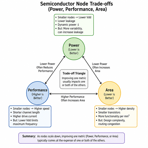
Every semiconductor node is a set of compromises. Designers constantly choose between speed, leakage, operating voltage, die area, yield, memory density, packaging cost, and thermal behavior. N3P’s value comes from giving design teams a better curve to work with, not from eliminating those trade-offs.
Performance versus leakage
Higher performance often comes with higher leakage or power draw. N3P’s stated improvement at the same leakage gives designers more headroom, but they still must decide how aggressively to use it. A mobile SoC may reserve that headroom for brief peak workloads, while an HPC design may use it to improve sustained throughput.
Logic density versus memory limits
Node shrinks tend to help logic more than some other structures. SRAM, analog, and I/O do not always scale at the same pace as digital logic. That means the practical density advantage of N3P depends heavily on the chip’s composition. A compute-heavy block may benefit differently from a chip dominated by cache or analog circuitry.
Manufacturing maturity versus bleeding-edge risk
A derivative node can be appealing because it builds on what came before. For large-volume products, manufacturing maturity matters almost as much as peak specifications. Better familiarity across design tools, IP libraries, process behavior, and packaging flows can help reduce uncertainty as a chip moves from tape-out to production.
How should companies evaluate TSMC nodes?
Companies should evaluate tsmc nodes by matching the node’s characteristics to the product’s real constraints, not by choosing the smallest number available. The right node is the one that delivers the best business and engineering outcome for the chip’s workload, schedule, volume, cost target, and power envelope.
A practical evaluation should include:
- Workload profile: Is the chip optimized for mobile bursts, sustained gaming, AI inference, networking, desktop performance, or data-center throughput?
- Power budget: Does the product need maximum peak speed, or is energy efficiency the primary goal?
- Thermal design: Can the end device remove heat effectively, or will the chip be limited by a thin smartphone chassis?
- IP readiness: Are the needed CPU, GPU, NPU, memory, interface, and security blocks ready for the node?
- Packaging strategy: Will the chip use package-on-package memory, advanced fan-out, chiplets, or other integration methods?
- Cost and yield expectations: Does the added performance or efficiency justify the design and manufacturing cost?
- Time to market: Can the team finish design, verification, validation, and ramp quickly enough to meet the product window?
This is why N3P is strategically important. It offers a refined option for teams that want advanced 3nm-class benefits without necessarily waiting for the next full node transition. In a market where smartphone generations, AI accelerator launches, and PC refresh cycles move quickly, that timing can be decisive.
N3P and the future of tsmc manufacturing
N3P also illustrates a broader shift in semiconductor innovation. The industry can no longer rely only on classic scaling to deliver dramatic improvements every generation. Instead, progress now comes from a combination of process refinement, design-technology co-optimization, advanced packaging, chip stacking, specialized accelerators, and software-aware architectures.
TSMC’s roadmap reflects that layered approach. The company continues to extend 3nm with variants such as N3P and N3X while also moving into 2nm-class technologies and beyond. TSMC has said its 2nm N2 technology uses its first-generation nanosheet transistor structure, with volume production starting in 2025 as planned.
That does not make N3P obsolete. Mature advanced nodes often remain valuable for years because they serve products that need proven manufacturing, rich IP support, and strong cost-performance balance. A flagship chip may move to the newest node first, but many high-volume designs benefit from staying on a refined process with predictable behavior.
Key takeaways for readers following N3P
N3P is best understood as an advanced, practical refinement of TSMC’s 3nm platform. It is not just a smaller label; it is a node designed to improve the choices available to semiconductor teams building demanding products.
The main points to remember are:
- N3P is part of TSMC’s 3nm FinFET family, positioned as an enhancement over N3E.
- Its value is in balanced PPA improvements, including speed, power, and density gains compared with N3E.
- It is highly relevant to premium mobile silicon, where power efficiency and thermal behavior matter as much as peak performance.
- It also supports HPC and AI design needs, especially where efficient compute density is a central goal.
- Real product gains depend on full-chip design, not the node alone.
- The node strengthens TSMC’s broader manufacturing ecosystem, giving customers another advanced option before or alongside migration to newer technologies.
The practical meaning of N3P innovation
The tsmc n3p node represents the kind of semiconductor progress that matters most today: incremental on paper, significant in products. A few percentage points of speed, power, or density can influence battery life, thermal stability, AI responsiveness, camera processing, and the competitive position of a flagship chip.
For engineers, N3P is a better design canvas. For product companies, it is a way to deliver more capable devices on a realistic schedule. For readers watching the semiconductor industry, it is a reminder that innovation is no longer only about the next headline node. It is also about how carefully refined tsmc manufacturing processes, smarter architectures, and mature ecosystems combine to keep modern computing moving forward.